FreeCore Function #14:
Dynamic RAM
Controller
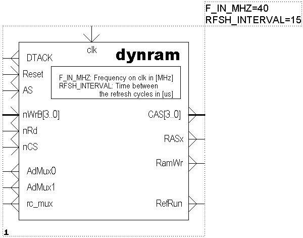
Module name: dynram
Current
release: version 1.1, January 1998
Contributed by: mailto:rodlerf@avl.com
Changes since version 1.0
Introduction
Dynamic RAMs are still the cheapest way to implement memory for microprocessor systems. But one fact is also that many hardware developers don’t like DRAMs in their designs, because DRAMs have the reputation to be critical in design. But it’s also a fact that many people hesitate to start a development of a suitable DRAM controller, because it costs a lot of time and does not bring the whole project further. As most processors doesn’t have a built in DRAM controller, they have to come along with static RAMs ... ! If there is a CPLD already planed in the new design, the DRAM controller can be easily added to the device.
Module description
The following module represents a DRAM controller for a 32 bit memory. It delivers a Data Transfer Acknowledge back to the processor and the necessary signals for the address multiplexer (CAS/RAS). It also generates a CAS before RAS refresh cycle, which can be parameterized.
PARAMETERS:
| F_IN_MHZ | Clock frequency in MHz (Default. 40MHz @ 60ns RAMs) |
| RFSH_INTERVAL | Time between two refresh cycles in m s. - e.g.: 2048 refreshes within 32ms: RFSH_INTERVAL=15 |
INPUT PORTS:
| Reset | Active HIGH reset signal |
| AS | Address Strobe, active LOW |
| nWrB[3..0] | Write, active LOW, for 4 bytes (32 bit memories) |
| NRd | Read, active LOW, for the whole Longword (32 bit) |
| NCS | Chip Select, active LOW |
| Clk | Clock (normally between 32 and 40 MHz @ 60-80 ns DRAMs) |
OUTPUT PORTS:
| DTACK | Data Transfer Acknowledge, active LOW, signals that the read data is valid, or that the data has been written. |
| AdMux0 | MUX out, RAS addresses to DRAM |
| AdMux1 | MUX out, CAS addresses to DRAM |
| rc_mux | RAS/CAS MUX for clocked multiplexing (becomes valid 1 cycle before AdMux[1..0] |
| RefRun | Refresh Running, only for info and simulation |
| RamWr | Write signal, for all DRAM chips (32 bit) |
| RASx | RAS signal, for all DRAM chips (32 bit) |
| CAS[3..0] | CAS signal, each for 1 byte (4 * 8bit) |
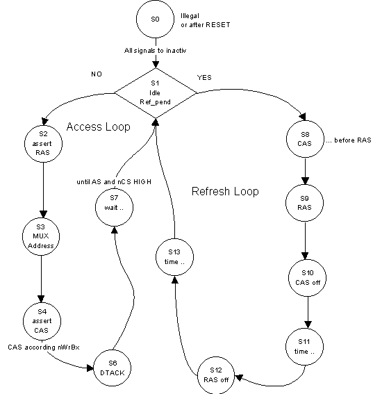
The flow chart
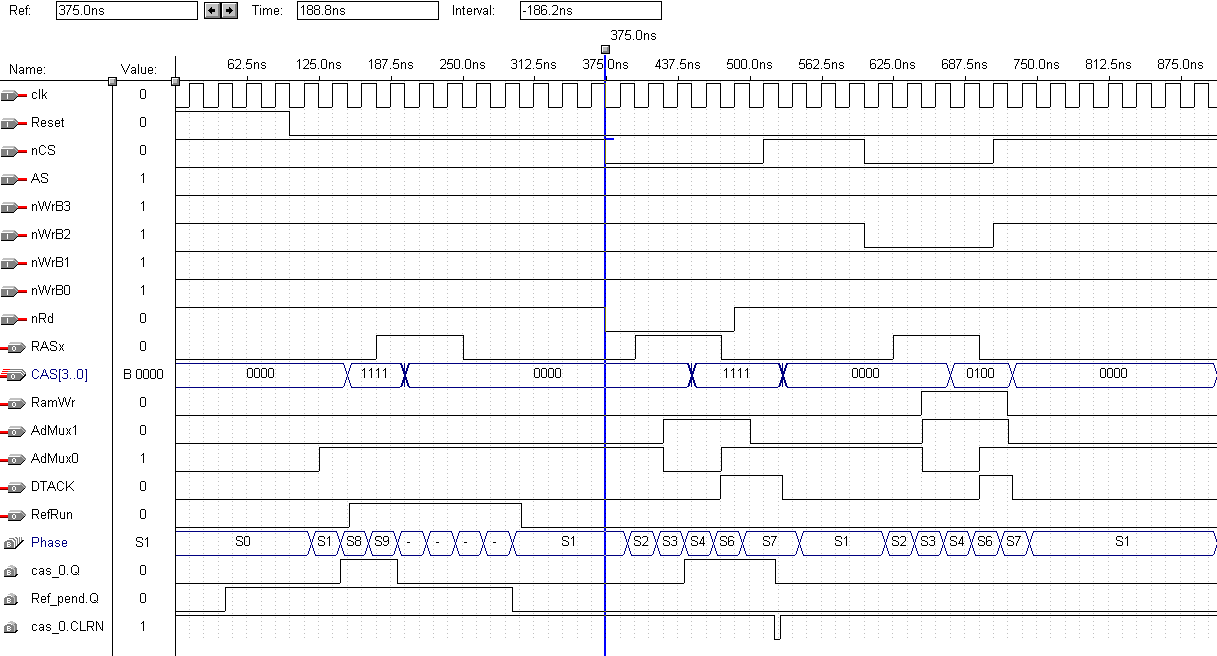
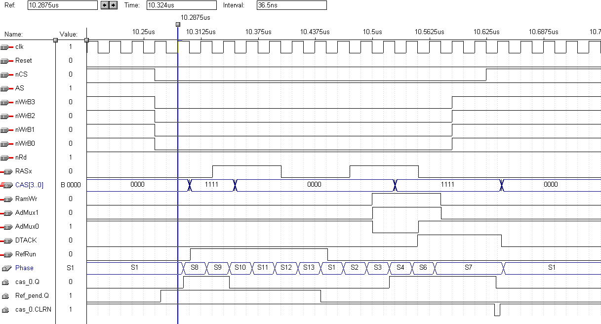
Some simulations
1) Simulation 1 shows the controller after a Reset. The first refresh takes
place followed by a read access.
The third access is a write to Byte-2.
Simulation 1
2) Simulation 2 shows the situation if an access (write to all 32 bits) happens at the same time as a refresh is pending. The refresh cycle wins and the normal access to the DRAM has to wait till the controller has reached S1.
Simulation 2
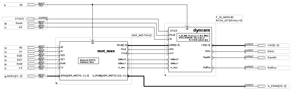
An application
Many popular processors don’t have a DRAM controller on-chip, so the MOTOROLA MC68030. The following application shows a possible interface to that processor.
Assumptions:
- RAM: 16Mbyte (4M*32)
- RAS: All chips to RASx
- CAS:
Every byte has it’s own CAS signal
- Write signal: All chips to RamWr
-
Clock: 40MHz
- RAM speed: 60ns FPM-DRAM; 2048 refreshes within 32ms
(RFSH_INTERVAL=15)
The mot_mux (included in the FreeCore Library) does the interface between the MC68030 and the DRAMs:
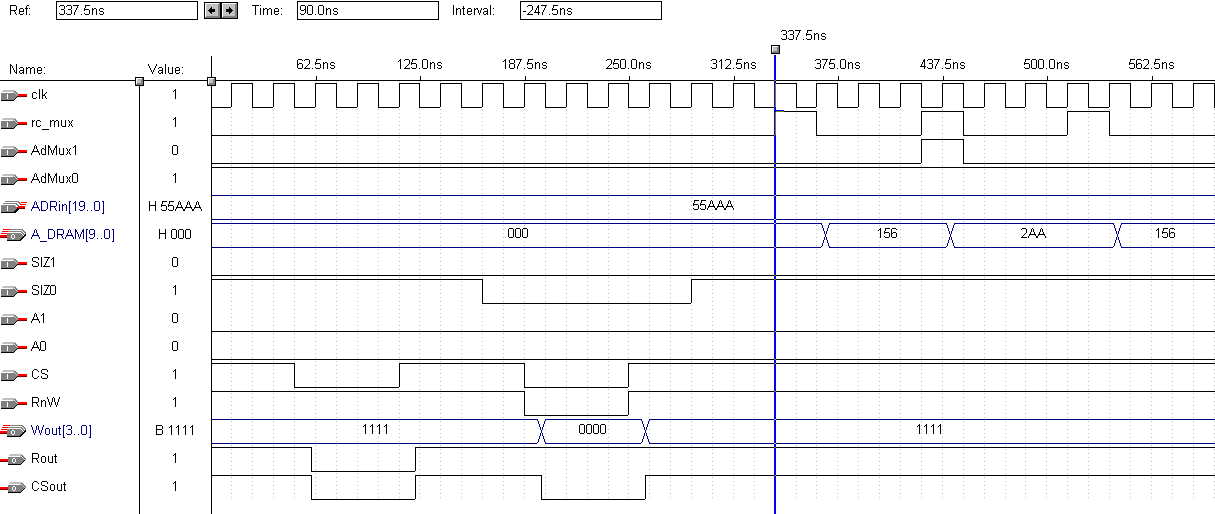
Some simulations
3) This simulation shows the behavior of the mot_mux module (e.g. 20 address lines)
Simulation 3
Hints for the choice of the right CPLD and ...
Address decoders and glue logic like that are in most cases implemented in non volatile logic (EEPROM). This has many reasons, but the most heard reason is a historical one: SRAM based glue logic is much to slow for modern processors (f_max ...) and the delay times are to large (e.g. >10ns ... ).
This DRAM controller is synchronous design and if the simulation attests a correct behavior at the wanted 40MHz, it should be no problem to implement this design into a SRAM based CPLD (e.g. 10Kxx-y). Well, ‘-3’ (10Kxx-3) chips should be used, otherwise it will be very hard for the compiler to hit the f_max target. In general, all chips with enough pins and healthy simulation can be used. The choice of the chip should depend on the functions which are added to the design. If only the main address decoder should be added, it will be wise to use a fast EEPROM based chip (e.g. 70xxx-10 or faster). But if an UART or another sequential function is needed, a SRAM CPLD is the better decision (price, redesigns etc.).
If the timing of this module with 40Mhz is to fast for the planed DRAM chips (more than 60ns), it’s possible to lower the clock frequency (to 32MHz) or to modify the state machine (insert wait states ... e.g S5).
External drivers and termination resistors
The shown design example (mot_mux) has an internal address multiplexer for the DRAM address lines (RAS and CAS addresses). If the design should be done in a similar way it’s recommended to put 33 Ohm resistors in series to the CPLD. Also use the resistors for the WRITE, RAS and CAS signals. If it is not wanted to use any external chips, an internal inverter between the RAS, CAS and WRITE output and the DRAM is necessary .
If an external multiplexer is preferred, a chip with controlled slow rate should be chosen (e.g. 74FCT2244). So the CPLD can save pins and become cheaper. But also in this configuration the 33 ohm resistor is a must!
Frank 01.98
![]()
Last updated 08 Feb 2001 11:53